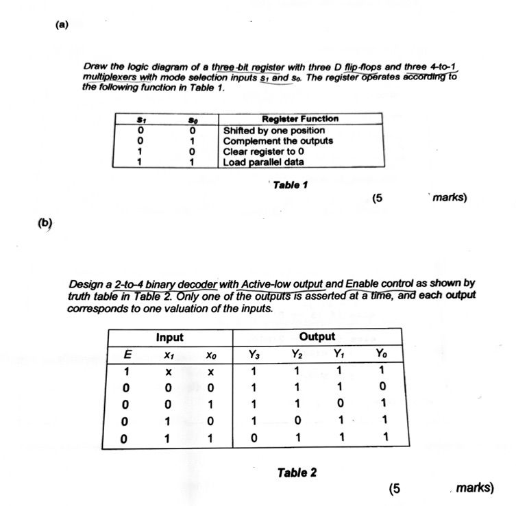
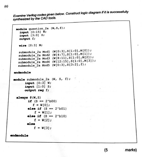
(Solved): (a) Draw the logic diagram of a three-bit register with three D flip-flops and three 4-to-1 multiple ...
(a) Draw the logic diagram of a three-bit register with three D flip-flops and three 4-to-1 multiplexers with mode selection inputs s, and so. The register operates according to the following function in Table 1. Table 1 (b) Design a 2-to-4 binary decoder with Active-low output and Enable control as shown by truth table in Table 2. Only one of the outputs is asserted at a time, and each output corresponds to one valuation of the inputs. Table 2 (c) Examine Verilog codes given below. Construct logic diagram if it is successfully synthesized by the CAD tools. ``` module question_2a (W,S,f); input [0:15] W; input [3:0] S; output f; wire [0:3] M; submodule_2a Mod1 (W[0:3],S[1:0],M[0]); submodule_2a Mod2 (W[4:7],S[1:0],M[1]); submodule_2a Mod3 (W[8:11];S[1:0],M[2]); submodule_2a Mod4 (W[12:15],S[1:0],M[3]); submodule_2a Mod5 (W[0:3],S[3:2],f); endmodule module submodule_2a (W, S, f); input [0:3] W; input [1:0] S; output reg f; always @(W,S) if ( }S==\mp@subsup{2}{}{\prime}b00\mathrm{ ) f = W[0]; else if (S == 2'b01) f = W[1]; else if (S == 2'b10) f = W[2]; else f = W[3]; endmodul ```