(Solved): Develop your 555 Timer to create a 1 Hz clock signal with a Duty Cycle as close to 50% as possible. ...
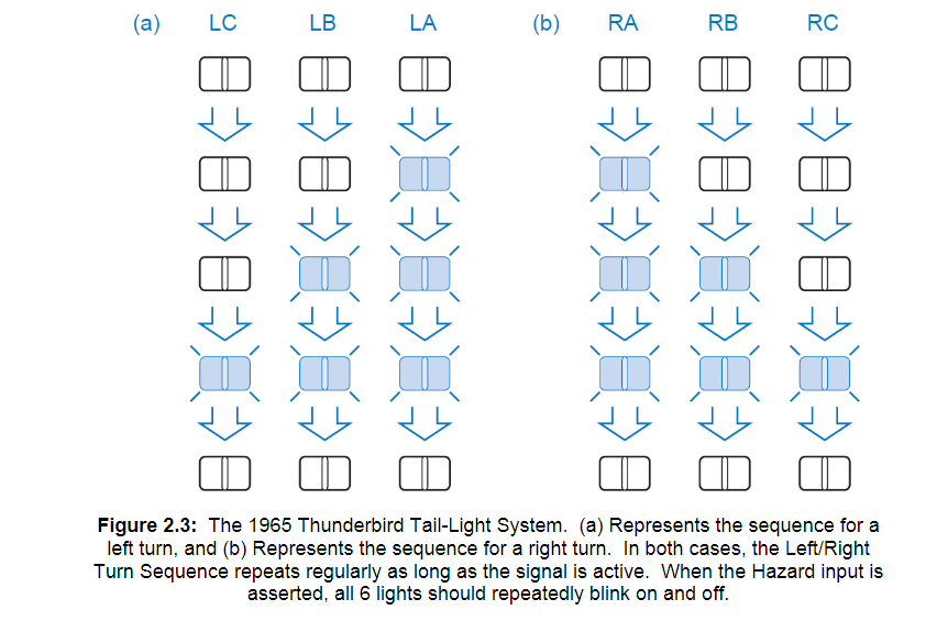
Develop your 555 Timer to create a 1 Hz clock signal with a Duty Cycle as close to 50% as possible. Determine the required resistor and capacitor values necessary to implement your design based upon the components in your lab kit. 4. Examine the specification sheet for the 74LS14 Schmitt Trigger Inverter. Draw a circuit diagram (with all necessary pinouts) that implements your 555 Timer and applies the Output of the Timer to the input of the 74LS14. Since the 7414 inverts your signal, use 2 inverters in series to buffer the clock. 5. After examining Figure 2.3, quantify the number of states necessary for the state machine, as well as the number of inputs and outputs to the system. Categorize the system as Mealy or Moore, again by observation. 6. Develop a State Diagram. 7. From the State Diagram, compute the (minimum) number of Flip-Flops required. 8. Assign each of the observable external states to an internal machine state (a unique Flip-Flop output combination). Although there are procedures for optimizing this assignment, for this exercise you may assign them arbitrarily. Page 5 of 6 9. Verify the State Diagram with your Instructor before proceeding any further. 4. LAB ASSIGNMENT 4.1 Synchronous State Machine Implementation 1. Once your State Diagram has been verified by your Instructor, produce a Next- State Table. Ensure that you design your machine to be self-starting, such that any used states have a valid and reasonable next state. As in lecture, the left- hand side of your Next State Table should possess the same number of columns as the Sum of the Present State Variables (Q0, Q1, etc.) and the number of inputs. The right-hand side of your Next State Table should possess the same number of columns as the Sum of the Next State Variables (Q0, Q1, etc.). 2. Assuming D Flip-Flops are used to create the memory cells, develop the Sum- of-Product Expressions (SOP) necessary to implement the Input Forming Logic to each of the Flip-Flops. The Input Variables used for your Input Forming Logic should include the external Inputs (Left, Right, and Hazard) as well as the Q/Q* outputs from each of the Flip-Flops, as necessary. The outputs for the IFL are the D inputs to the Flip-Flops. 3. Minimize the IFL SOP expressions using K-Maps to simplify the logic needed to implement the Input Forming Logic. 4. Develop the necessary Output Forming Logic from the output of your States to drive 6 LEDs. Minimize the expressions, as necessary. 5. Examine the ATMEL ATF750C Specification Sheet, ATMEL WinCUPL User’s Manual, and WinCUPL Tutorial to determine how to create the necessary source code to implement your Synchronous State Machine. 6. Compile your source code to create a JEDEC output file, which can then be used to program the ATMEL ATF750C using the ATEMEL Device Programmer. When programming your devices, be sure to use the anti-static wrist band to ground yourself, since the CMOS chips are easily damaged by static electricity. 7. Develop a Complete Circuit Diagram (with full pinouts for each chip) for your Synchronous State Machine design. 8. Build and test your system, using your circuit diagram as a guide. Note that the final output of your Synchronous State Machine should drive 6 LEDs to emulate the Tail-Light Section of the 1965 Thunderbird. Use switches for the Boolean Page 6 of 6 Inputs (LEFT, RIGHT, HAZARD), and the output of the 555 Timer (buffered by the 7414 Inverters) as your Input Clock. 9. Demonstrate your working circuit to your instructor. 10. Document your entire design process.