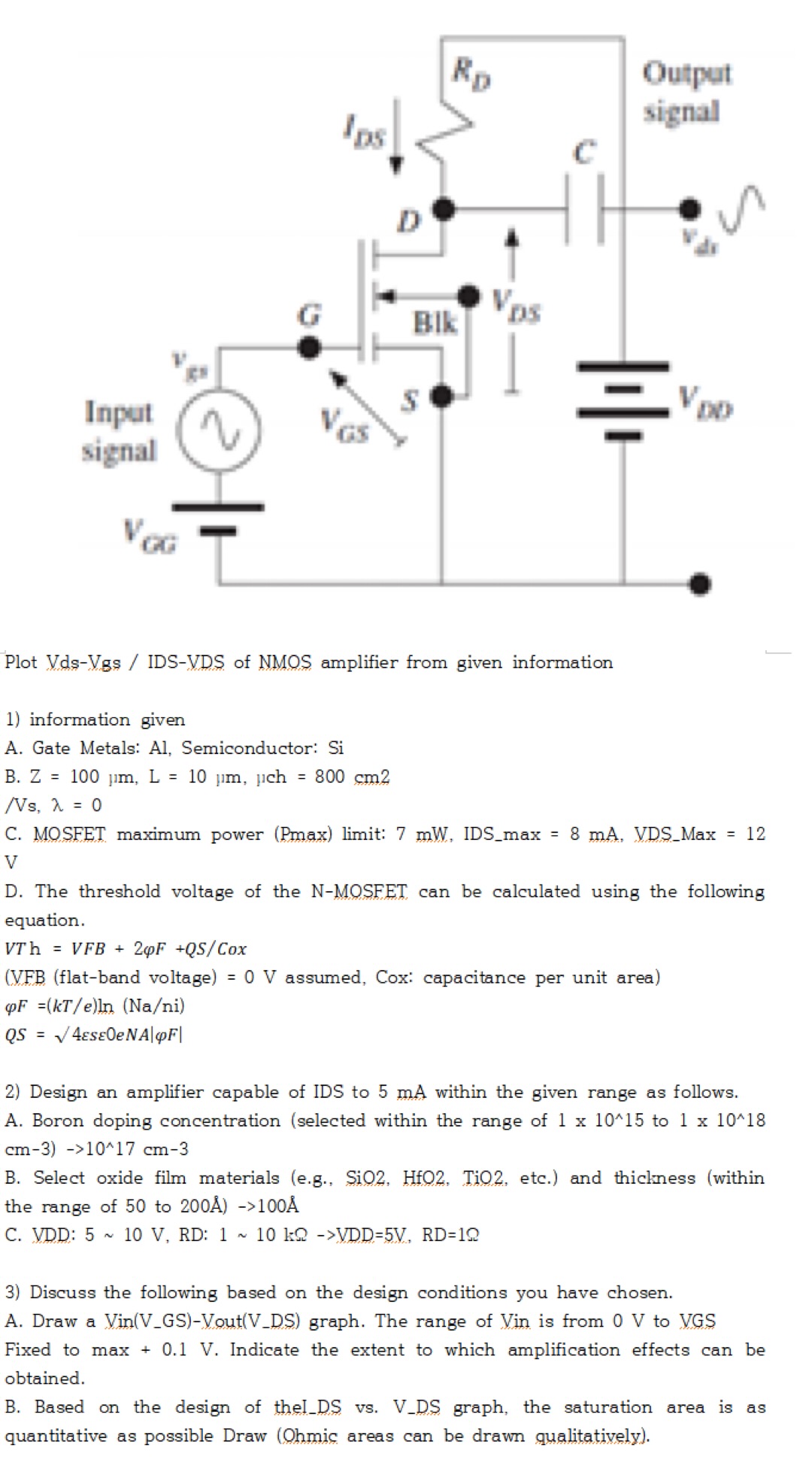
(Solved): Plot Vds-Vgs / IDS-VDS of NMOS amplifier from given information information given A. Gate Metals: A ...
Plot Vds-Vgs / IDS-VDS of NMOS amplifier from given information information given A. Gate Metals: Al, Semiconductor: Si B.
Z=100\mu m,L=10\mu m,\mu ch=800cm2/Vs,
\lambda =0C. MOSFET maximum power (Pmax) limit:
7mW, IDS_max
=8mA, VDS_Max
=12
VD. The threshold voltage of the N-MOSFET can be calculated using the following equation.
VTh=VFB+2\phi F+Q(S)/(C)ox(VFB (flat-band voltage)
=0Vassumed, Cox: capacitance per unit area)
\phi F=(k(T)/(e))ln(N(a)/(n)i)
QS=\sqrt()4\epsi s\epsi 0eNA|\phi F|Design an amplifier capable of IDS to
5mAwithin the given range as follows. A. Boron doping concentration (selected within the range of
1\times 10^(15)to
1\times 10^(18)
cm-3B. Select oxide film materials (e.g.,
SiO2,HfO2,TiO2, etc.) and thickness (within the range of 50 to
200\angstrom )
->100\angstrom C. VDD:
5?10V,RD:1?10k\Omega ->VDD=5V,RD=1\Omega Discuss the following based on the design conditions you have chosen. A. Draw a Vin(V_GS)-Vout(V_DS) graph. The range of Vin is from
0Vto VGS Fixed to max
+0.1V. Indicate the extent to which amplification effects can be obtained. B. Based on the design of theI_DS vs. V_DS graph, the saturation area is as quantitative as possible Draw (Ohmic areas can be drawn qualitatively).