(Solved): Problem 2: p-i-n Diode A p-i-n diode is a semiconductor diode with a wide, lightly doped intrinsic r ...
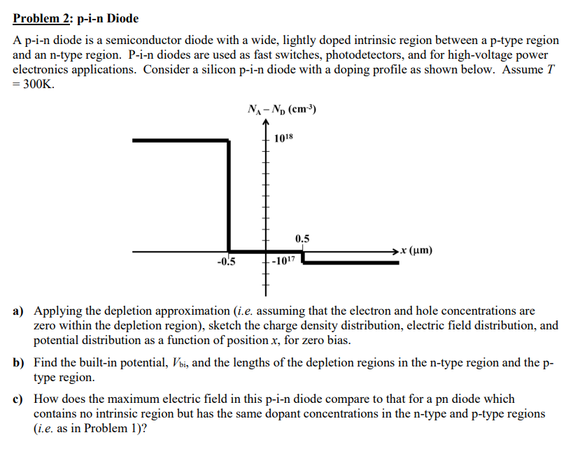
Problem 2: p-i-n Diode A p-i-n diode is a semiconductor diode with a wide, lightly doped intrinsic region between a p-type region and an n-type region. P-i-n diodes are used as fast switches, photodetectors, and for high-voltage power electronics applications. Consider a silicon p-i-n diode with a doping profile as shown below. Assume \( T \) \( =300 \mathrm{~K} \). a) Applying the depletion approximation (i.e. assuming that the electron and hole concentrations are zero within the depletion region), sketch the charge density distribution, electric field distribution, and potential distribution as a function of position \( x \), for zero bias. b) Find the built-in potential, \( V_{\mathrm{bi}} \), and the lengths of the depletion regions in the n-type region and the ptype region. c) How does the maximum electric field in this p-i-n diode compare to that for a pn diode which contains no intrinsic region but has the same dopant concentrations in the n-type and p-type regions (i.e. as in Problem 1)?